Semiconductor / Battery
WLP(Wafer Level Package) AOI
Next-Generation Wafer-Level Package Inspection Equipment with Integrated 2D/3D Optics
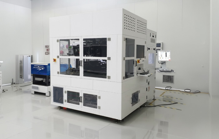
We provide high-precision AOI equipment designed to relably detect
micro-scale defects in wafer-level packaging processes. By combining
optimized lighting with AI-based deep learning, the system enhances
detection performance and improves yield through integrated inspection workflows.
-
Precision optical inspection of 2D/3D defects in wafer-level packaging processes
-
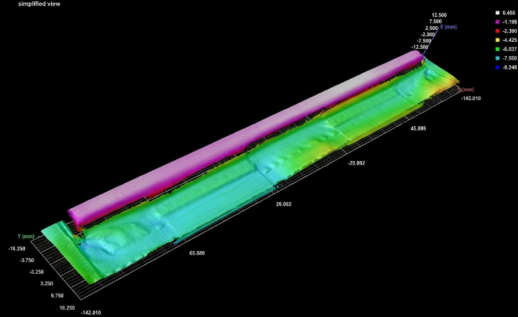
Advanced inspection logic for RDL(redistribution layer) patterns and bump height/shape
-
Enhanced image contrast and improved detection of fine defect through optimized lighting
-
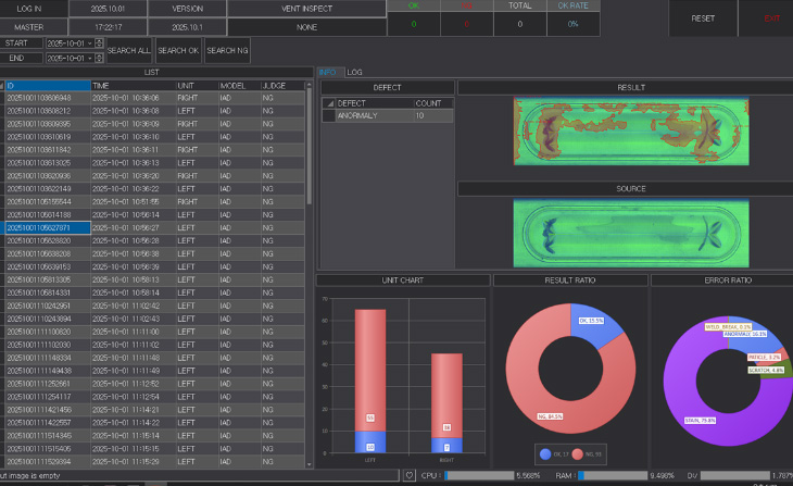
AI-based real-time defect classification and inspection decision-making
-
High-speed processing and reliable data performance for semiconductor production lines
Battery inspection equipment
End-to-End Quality Assurance with Integrated Control and 2D/2.5D/3D High-Speed Optical Inspection
We provide high-speed inspection equipment optimized for every stage of battery manufacturing, from electrode processing to final module
and pack assembly. By integrating 2D AOI, 2.5D(Photometric Stereo), 3D profiling, and AI-based analysis, the system enables
precise defect detection and improved production yield.
-
Electrode Process : High-speed surface inspection for contamination, pinholes, stains, and scratches
-
Cell Assembly Process : Precision inspection of alignment, dimensions, step height, and 3D shape(2.5D/3D)
-
Welding&Sealing Process : Combined 2D and 2.5D inspection for weld quality, shape anomalies, and surface defects
-
Module & Pack Process : Inspection of cell height, flatness, spacing variation, and key assembly features
-
Line Integration : PLC/MES integration, image and log data traceability, and AI-based automated classification